| Home | Web Design | Programming | Fairlight CMI | Soap Box | Downloads | Links | Biography | About... | Site Map |
|
FAIRLIGHT TECHNOLOGY |
| Fairlight CMI |
Examples | Swap Shop | Messageboard | Tales | Images | Wild | [Technology] | Voicetracker |
News Flash |
· GH Services is the North American distributor for BassLab of Germany.
Click here
for these unique guitars and basses. · Horizontal Productions repairs and upgrades Fairlight CMIs from Series I to MFX2. Visit http://www.horizontal.co.uk/. |
|
FAIRLIGHT CMI |
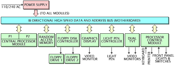
The Fairlight CMI is built on the QASAR business computer, which was designed as a general purpose computer suited for commercial and scientific data processing, program development, and many other applications. The QASAR has a dual-processor architecture, with two microprocessors operating simultaneously on the same bus. This allows one processor to be dedicated to polling and buffering input, while the other runs the application. Add-in cards include the processor controller, floppy controller,
memory-mapped video card, and a 64K memory card. All of the cards use
standard discrete electronic components, with no custom chips. The
typical Motorola support chips are used, including 6880, 6850, 6840,
and 6821. Others include those by Texas Instruments, National
Semiconductor, Harris, and Intel. |
|
Two processor cards are available: one with dual Motorola 6800 processors (used in the CMI Series I and II), and a 6800/6809 version (for the IIx). The two processors run interleaved on a 1 MHz common bus, resulting in a 2 MHz bus. In the standard configuration, P1 is an I/O processor (handling keyboard, screen, printer, and time-of-day updating) while P2 executes user programs and disk access. The machine can be thought of as a single-processor computer attached to a sophisticated terminal.
QASAR RAM cards have a cycle time of 500 ns, ensuring that the two CPUs can access memory without contention. The 64K memory cards allow separate 16K blocks of physical memory to be programmatically assigned to any 16K boundary in the address space of either, nether, or both of the processors (memory can be made common for inter-processor communications). Each processor can access more than 64K by switching different blocks in and out of the same address space. A DIP switch on each memory card provides a unique identifier, but card 0 is the only one used by the system, leaving the rest for user programs. It is theoretically possible to provide up to 1 megabyte of RAM, even though the 6800 can only address 64K bytes directly.
The memory map of the QASAR reflects hardware (processor controller and screen output cards) and I/O options. The top 4K of memory space ($F000-$FFFF) is located on the Processor Controller card, and performs specialized systems functions, such as serial and parallel I/O, floppy disk operations, processor interaction, and program debugging. The rest of the address space ($0000-$EFFF) is used by QDOS and user programs. The diagram "MEMORY MAP AT STARTUP" shows the memory as configured by the firmware at power-up or restart. The ROMs, located on the Processor Controller card, provide a debug monitor program as well as routines for peripheral and floppy I/O. The debug monitor is entered by pressing the console interrupt button, which sends an NMI (non-maskable interrupt) to processor 2, halting the program. With the text terminal option (TVT) installed, P1 RAM is available from $8000 to $E000. With the 16K graphics board installed, and when P1 is running the optional software interface toolkit called the IOPACK, the screen is converted into a graphics terminal, which allows vector and point potting, protected field I/O, and light-pen functions. P1 RAM above $8000 is unavailable in this mode.
A user program may be run in P1 by loading it into common memory and storing the start-of-execution address in $FE01 (hi byte) and $FE02 (lo byte).
Differences between the dual 6800 and the 6800/6809 system are fairly small, but significant, meaning that programs created for the dual 6800 system may not run on the 6800/6809 without modifications. After restart, the 6809 functions as processor 1, waiting in a loop, while processor 2 runs the disk operating system and other 6800 programs. The 6800 handles disk and peripheral I/O without queueing, just as a single-processor computer would. The QDOS LOAD command with the "UG" option can load a 6809 program into any area of common memory and run it. The "U" option causes the 6800 to be reconfigured to operate an as I/O processor for the 6809. All calls to OS or ROM subroutines from the 6809 are automatically executed by the 6800, which provides I/O compatibility and allows many existing 6800 programs to be run on the 6800/6809 system with few changes. The Processor Controller card provides one serial input, two serial outputs, and two 8-bit bi-directional parallel ports. Normally, the serial input is used by the keyboard and one serial output controls a printer. 8" x 8" cards plug into the motherboard/backplane, which provides data, address, timing, control, and power supply lines. The power supply provides 5 V at 10 A (15 A optional) and +/- 12 V at 1.0 A (1.5 A optional). All floppy disk operations are handled by DMA through the floppy disk controller module and routines in P2's unique ROM. Each DMA cycle is achieved by stretching P2 clock phase 1 by one microsecond, making DMA completely transparent to the processors and saving the time to do the usual req/ack cycle. A user program normally accesses the floppy disks by calls to QDOS, which maintains file directories and sector buffers. QDOS supports single- and double-sided disks with a capacity of 250K and 500K, respectively. Up to 160 files may be stored on each disk, and files may range in size from 512 bytes (4 sectors) up to the maximum capacity of the disk. ...more to come.. |
||||||||||||||||||||||||||||||||||||||||||||||||||||||||||||||||||||||||||||||||||||||||||||||||||||||||||||||||||||||||||||||||||||||||||||||||||||||||||||||||||||
| Home | Web Design | Programming | Fairlight CMI | Soap Box | Downloads | Links | Biography | About... | Site Map |
| Send comments about this site to Greg at
ghservices.com@gmail.com All trademarks contained herein are the property of their respective owners All pages copyright © 1996-2008 GH Services™ Created 2003-11-20 Last updated 2024-02-13 |